

Superconducting Fabrication Platform
SC Layer & Dielectrics Patterning

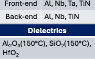
Layer Stack
Wafer-Scale Superconducting Layers
iQnite provides wafer-scale 2D superconducting fabrication for quantum devices and microwave circuits. Our platform supports superconducting base-layer materials including Al, Nb, Ta, and TiN, with TiN kinetic inductance available up to 60 pH/sq for compact, high-impedance circuit designs.
Integrated dielectric films
Al₂O₃, SiO₂, and HfO₂ support
Low-temperature Al₂O₃ and SiO₂ deposition
Temperature-sensitive device integration
Fabrication Flow
From Surface Prep to Patterned Devices
Supports CPW resonators, parallel-plate capacitors, quantum amplifiers, and planar microwave circuits.
Surface Cleaning
Prepare wafer surfaces for reliable superconducting film formation and downstream patterning.
Thin-Film Deposition
Deposit superconducting base layers and integrated dielectrics for quantum and microwave circuit fabrication.
Lithography
Pattern device features through photolithography and electron-beam lithography.
ICP-RIE Dry Etching
Transfer patterns with high-quality dry etching for superconducting device structures.